| English | Japanese |
|
Yesterdays access |
|
| Page Top | [Lily Diary.】 A diary of life in Mindanao. |
| 26/11/07 | SatBox_Ver0.1.1c-beta IC-9700 Test Version |
| 26/11/07 | SatBox User Guide |
| 26/11/03 | An FT-847 for SatBox Development |
| 26/11/02 | Buying a ZT219 Digital Multimeter |
| 26/10/28 | Building a home server using Linux |
| 26/10/27 | Repeater Controller Features and Settings |
| 26/10/27 | Repeater Controller Board and Firmware |
| 26/10/26 | JTDX Auto Run Ver0.7.7 |
| 26/10/26 | WSJT-X Auto Run Ver0.1.6 |
| 26/10/22 | Memories of UNIX and Networking from My Yonezawa Ham Shack |
| 26/10/20 | Acquiring a YAESU FT-2600M for a Repeater |
| 26/10/19 | Rotator Relay Interface for Sale |
| 26/10/18 | Kenpro Rotator Interface KiCAD DATA |
| 26/10/17 | JOTA in Indonesia: Jamboree on the Air |
| 26/10/17 | You Can Now Leave Comments |
| 26/10/11 | Installing Arduino IDE |
| 26/10/09 | DXCC200 Sticker Arrives from ARRL |
| 26/10/08 | SatBox Cloud Released |
| 26/10/06 | Bought an ECS LIVA Z Mini PC on Yahoo Auctions |
| 26/10/05 | QSO with C5R in The Gambia |
| 26/10/04 | Installing Raspberry Pi OS |
| 26/10/02 | Repeater Controller Features and Settings |
| 26/10/01 | Repeater Controller Board and Firmware |
| 26/09/30 | Ordering PCBs and Assembly from JLCPCB |
| 26/09/24 | UNITRUST Electronics Parts Shop |
| 26/09/22 | Kenpro Rotator Interface |
| 26/09/18 | SatBox KiCad PCB and firmware |
| 26/09/14 | designed a circuit board for SatBox |
| 26/09/12 | Solar Power System Plan |
| 26/09/09 | Satellite SatBox Part 4 |
| 26/09/04 | My grandson Zion |
| 26/08/29 | Ham Fair 2026 to be held |
| 26/08/25 | QSO with RI1FJL from Franz Josef Land |
| 26/08/23 | Satellite QSO via RS-44 |
| 26/08/22 | Currently, Satellite VUCC46 |
| 26/08/16 | Satellite SatBox Development in Progress - Part 3 |
| 26/08/05 | IC-820H Receiver Sensitivity Test |
| 26/08/02 | Satellite SatBox Development in Progress - Part 2 |
| 26/07/16 | Delivery of the 3D printed panels |
| 26/07/09 | Development of SatBox for satellites |
| 26/07/05 | Weather Monitor Indoor Unit |
| 26/06/30 | Creating data for 3D printers using FreeCAD |
| 26/06/16 | Installing an AS5600 magnetic encoder on a KR-500. |
| 26/06/05 | Grandson Zion's CQ |
| 26/06/04 | Replacing the potentiometer on the KR-500 elevation rotator |
| 26/06/03 | Making a Repeater Controller Pert4 |
| 26/06/01 | Weather Monitor software |
| 26/05/31 | Weather Monitor |
| 26/05/21 | JTDX Auto Run BUGFIX |
| 26/05/17 | Repair of satellite antenna system |
| 26/05/13 | Repair of Alinco DR130 |
| 26/05/07 | Making a Repeater Controller Pert3 |
| 26/05/03 | Indonesian satellite friend YC8RPK |
| 26/04/26 | DXCC200 achieved |
| 26/04/23 | Communication via ISS voice repeater |
| 26/04/20 | WSJT-X Auto Run Ver0.1.5 |
| 26/04/19 | Got an Alinco DR-130 |
| 26/04/15 | Clublog Charts |
| 26/04/10 | Regarding POC transceivers |
| 26/04/08 | Using KENWOOD AT-300 with YAESU radio |
| 26/03/17 | How to establish a radio club in the Philippines |
| 26/03/10 | KENWOOD AT-300 with YAESU radio |
| 26/02/27 | Philippine NTC Amateur Radio License Examination Question Bank |
| 26/02/20 | Package received from JK1SNS |
| 26/02/18 | Temporary License Renewal |
| 26/02/14 | Satellite Tracking Software SatTrack |
| 26/02/05 | Making a Repeater Controller Pert2 |
| 26/02/02 | CQ on satellite IO-86 |
| 26/01/27 | Shack & Repeater Controller |
| 26/01/16 | Making a Repeater Controller |
| 26/01/16 | Making aRotator Interface PCB |
| 26/01/10 | Satellite antenna installation |
| 26/01/08 | WSJT-X Remote Operation |
| 26/01/07 | JTDX Remote Operation |
| 26/01/04 | log_reciver_Ver2.6.6 |
| 26/01/04 | Tailscale VPN software for JTDX_Remote |
| Online Multiple Choice Reviewers to the Phil Amateur Radio Examination by 4F3EW A joint project by JI1FGX/DU9 and DV9JRD |
| Ordering PCBs and Assembly from JLCPCB (September 30, 2026) | ||||||||||||||||
|---|---|---|---|---|---|---|---|---|---|---|---|---|---|---|---|---|
|
I used KiCad to design the SatBox schematics and printed circuit board. The version used was KiCad 10.0.1 (release build). KiCad is free and feature-rich, but I initially found it difficult to learn how to use it. I worked through the design by asking ChatGPT for help whenever I was unsure about an operation. This page uses SatBox as an example to explain how to order PCB fabrication and surface-mount assembly from JLCPCB. The screenshots and prices are from this order.
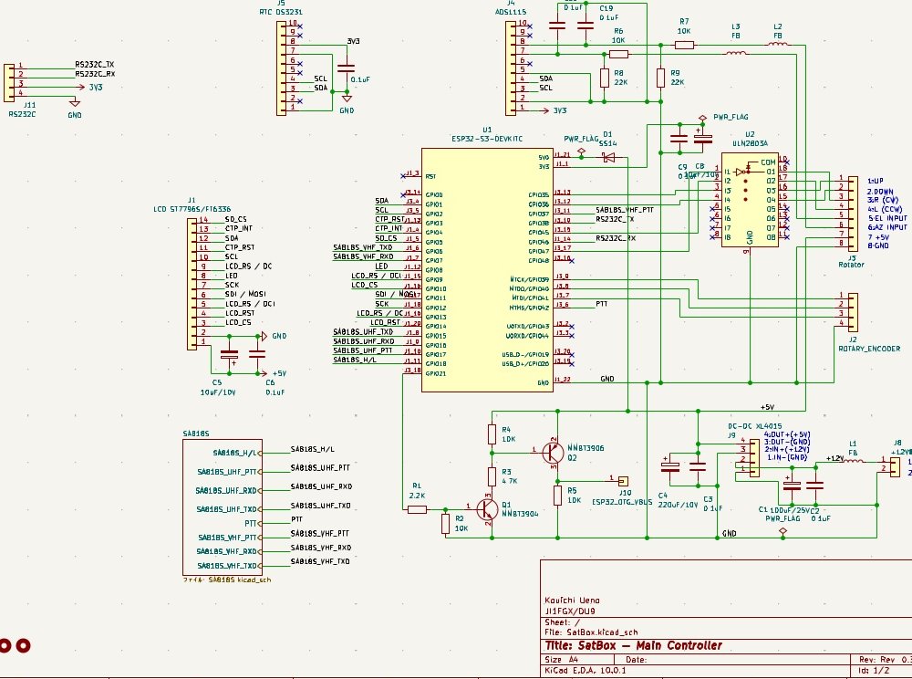 Figure 1. SatBox digital schematic, including the microcontroller, clock, display, and touch input circuits. | ||||||||||||||||
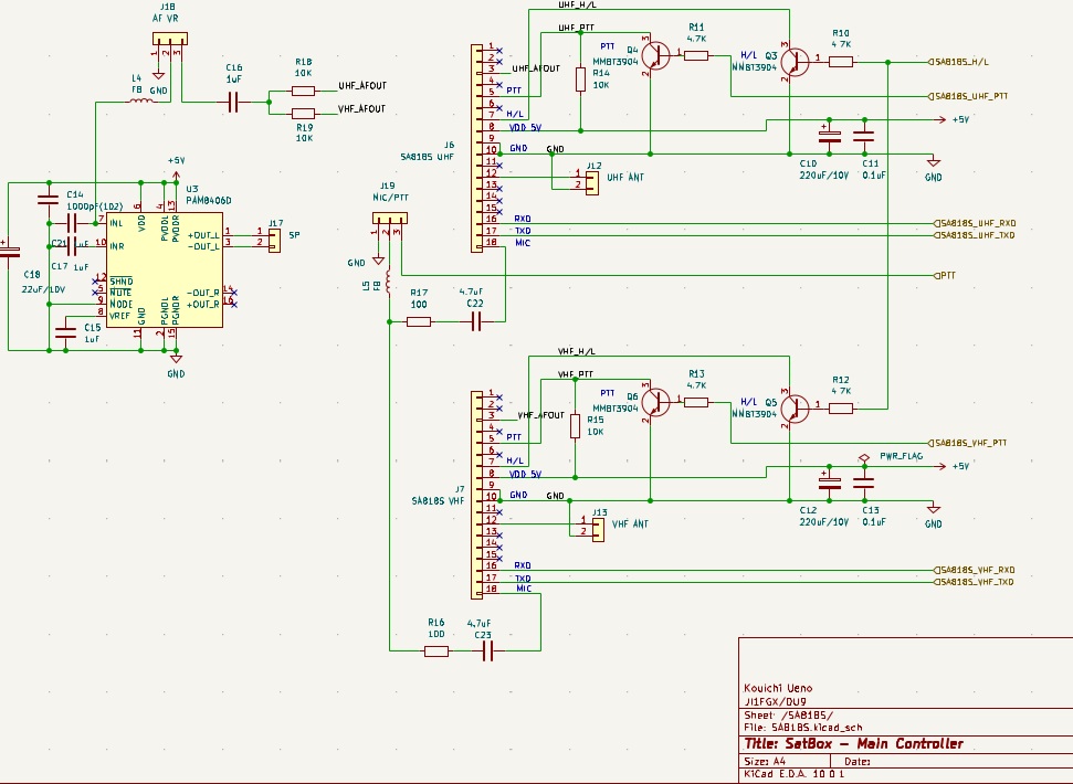 Figure 2. SatBox radio and audio schematic, showing the circuitry around the VHF/UHF modules and audio amplifier. | ||||||||||||||||
|
Next, I designed the board in the KiCad PCB Editor. After placing the components, I used the Freerouting external plugin to route the board automatically. Automatic routing still requires careful review and manual adjustments. 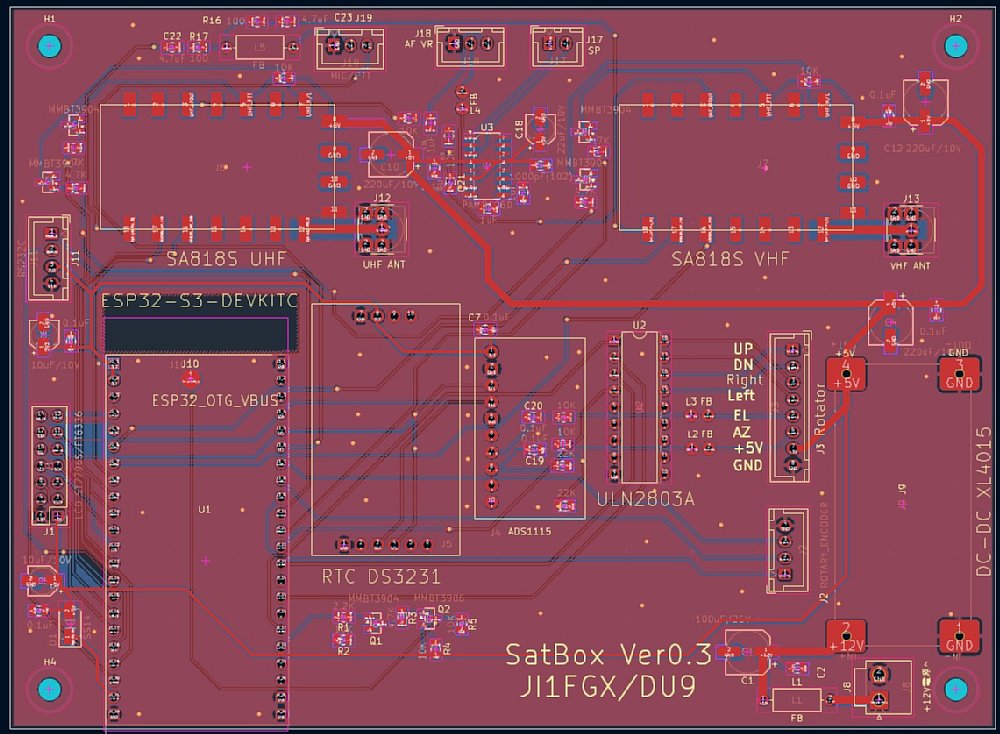 Figure 3. PCB layout created in the KiCad PCB Editor. | ||||||||||||||||
| For this order, JLCPCB will assemble the surface-mount components. Components that I will solder by hand are excluded from the assembly data. In the footprint properties for each of these components, select "Exclude from position files" and "Exclude from bill of materials." 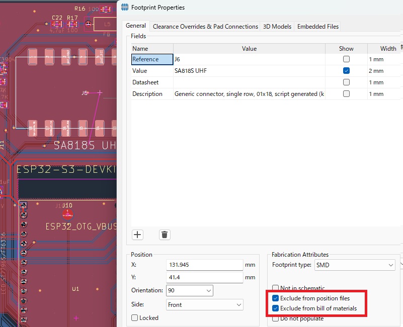 Figure 4. Settings to exclude hand-soldered components from the BOM and component position files. | ||||||||||||||||
|
Open Tools → External Plugins → Fabrication Toolkit. This plugin exports the files needed for PCB fabrication and assembly, including Gerber files, the BOM, and component placement data. 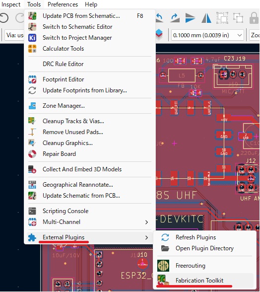 Figure 5. Launching Fabrication Toolkit from the external plugins menu in KiCad. | ||||||||||||||||
Review the Fabrication Toolkit settings, then click Generate to create the files.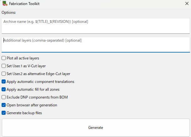 Figure 6. The Fabrication Toolkit export window. Click Generate to create the output files. | ||||||||||||||||
|
Go to the JLCPCB quotation page and upload the ZIP archive containing the Gerber files generated by Fabrication Toolkit. For this order, I uploaded SatBox.zip. 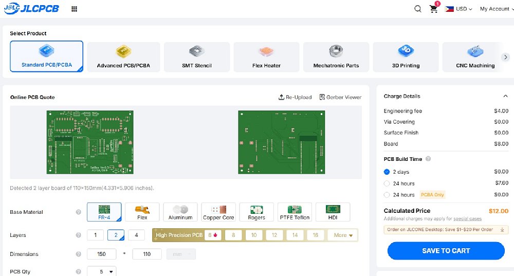 Figure 7. The JLCPCB quotation page. Upload the Gerber files and review the board specifications. | ||||||||||||||||
Enable PCB Assembly to have JLCPCB assemble the surface-mount components as well as fabricate the boards.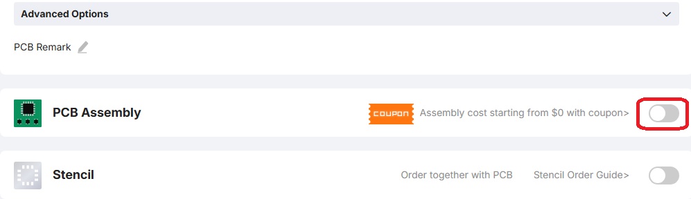 Figure 8. Enabling PCB Assembly to order component assembly along with PCB fabrication. | ||||||||||||||||
Check the assembly side and quantity. Select Yes for the component placement confirmation option, then click Next.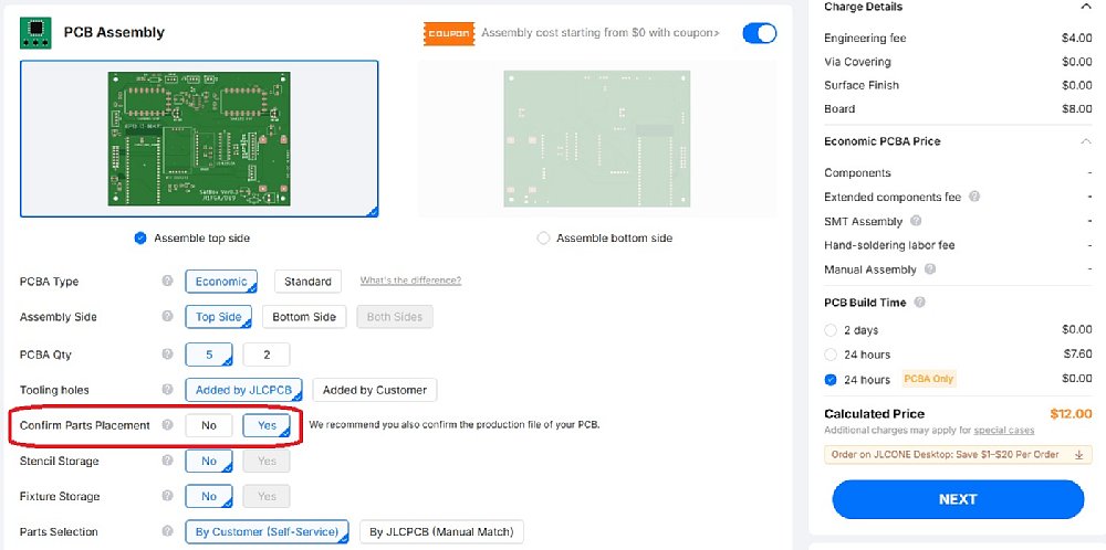 Figure 9. Example assembly settings: top side, five boards, and component placement confirmation enabled. | ||||||||||||||||
Review the board preview, then click Next.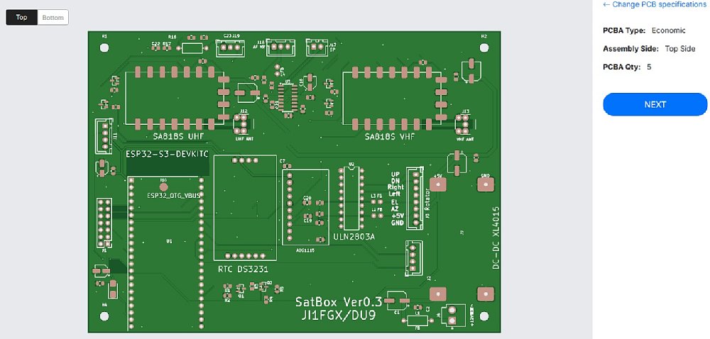 Figure 10. The board preview generated from the uploaded files. | ||||||||||||||||
Upload the BOM and CPL files. Once both files are selected, click Process BOM & CPL.
 Figure 11. The BOM and CPL upload fields. Select the bill of materials and component placement file separately. 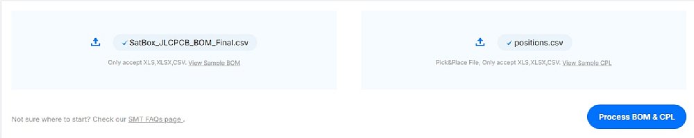 Figure 12. Both files have been selected. Click Process BOM & CPL to continue. | ||||||||||||||||
|
On the next screen, match the components in the uploaded BOM to the JLCPCB parts catalog and confirm the parts to be assembled. The left side shows the component references, values, and footprints from the design. The right side shows the corresponding part numbers, specifications, required quantities, and prices. Check that resistance, capacitance, voltage ratings, package sizes, and other specifications match the design. 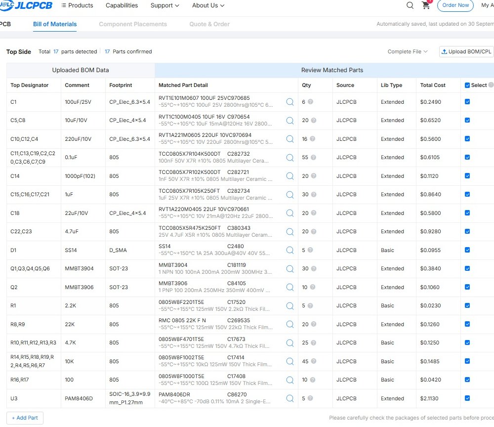 Figure 13. BOM matching results. Review the selected part numbers, specifications, and quantities. I also used ChatGPT to help find alternative part candidates. 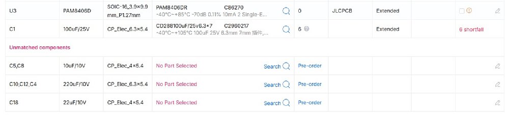 Figure 14. Examples of insufficient stock and unmatched components that require further review. | ||||||||||||||||
|
This preview shows the surface-mount components placed on the board. Check that component positions, orientations, and polarities match the design. 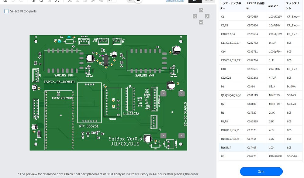 Figure 15. Board preview showing the components selected for assembly. | ||||||||||||||||
Review the PCB fabrication and assembly (PCBA) quotation, then click Save to Cart.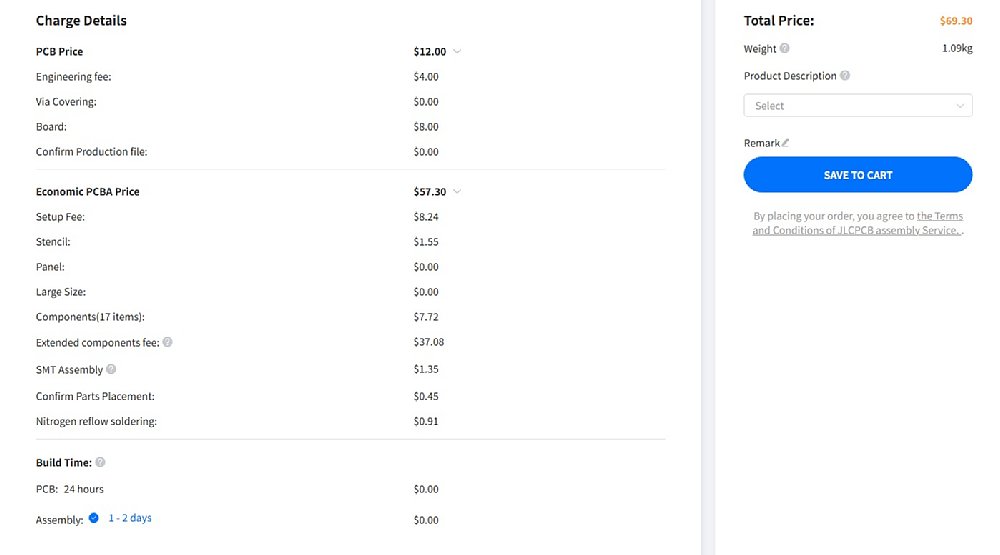 Figure 16. Reviewing the quotation for PCB fabrication and assembly. | ||||||||||||||||
|
Review the order details and quotation in the cart. For this order, fabrication of five boards cost US$12.00 and PCB assembly (PCBA) cost US$57.30, bringing the item subtotal to US$69.30. Adding US$10.02 for shipping and subtracting a US$10.00 coupon discount gives a displayed total of US$69.32. After checking the order details, click Secure Checkout to proceed with payment and place the order. 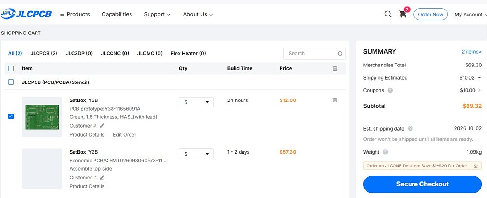 Figure 17. The shopping cart. The displayed total is US$69.32 after shipping and the coupon discount. | ||||||||||||||||
| September 24, 2026 October 1, 2026 | ||||||||||||||||